


The optimization effect of microwave plasma surface treatment on Die Bond and Wire Bond
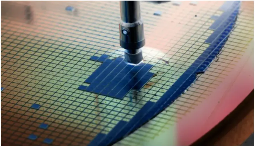
Today, we will mainly discuss the impact of cleanliness. During the packaging process of semiconductor chips, the cleanliness of the material surface is a crucial factor, as it directly affects the electrical connection between the chip and the substrate, thereby impacting the reliability and stable operation of the chip.
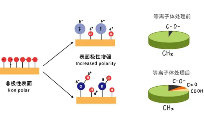
Plasma cleaning is a method that utilizes high-frequency electric fields to excite plasma for cleaning material surfaces. It can effectively remove organic substances, oxides, moisture, and impurities from the material surface, as well as improve the surface energy of the material, enhancing its wettability and providing good optimization for die attach and wire bonding processes.
The excitation frequency of microwave plasma can reach 2.45 GHz, which, compared to RF and intermediate frequency plasmas, has a higher plasma density. This results in a greater number of ions and a higher concentration of free radicals, allowing for effective cleaning primarily through chemical reactions. Additionally, with a relatively lower self-bias, microwave plasma also incorporates gentle physical reaction cleaning, which does not cause physical damage or heating issues to the substrate material.
Through microwave plasma surface treatment, not only can the cleanliness of the substrate surface be improved and the chemical properties of the material surface altered, but it can also enhance the affinity between the chip and the substrate surface, strengthen the bonding force between the metal and the substrate, and improve the reliability and durability of the packaging. Furthermore, it can regulate the energy state of the substrate surface and the distribution of chemical groups, making the adhesion and connection processes of Die Bond and Wire Bond more stable and controllable.
In recent years, with the development of packaging technology, plasma cleaning has been widely used in various process steps of semiconductor chip packaging. High-performance microwave plasma cleaning equipment has gradually opened up the market, leading to more application scenarios and fields, such as in the cleaning of power semiconductors, silicon carbide chips, semiconductor lasers, optical communication modules, optoelectronic sensors, and material manufacturing.
During the cleaning process of sensitive chips and high-precision surfaces, microwave plasma cleaning proves to be highly effective, significantly improving and optimizing the subsequent packaging steps and the overall packaging quality.
Contact Us
For any questions regarding our products or solutions, kindly entrust them to us and we will respond within 24 hours.
KeyWords
Wedge Bonding ToolWedge Tool
Bonding Wedge
Au Wire Bonding
Concave wedge Tool
Wedge Bonding Machines
Wire Bonding ToolsBonding Equipment SuppliersFine Pitch Bonding ToolsWedge BonderWire bonding equipmentSemiconductor bonding toolsPrecision bonding toolsHigh-performance wire bonding toolsSemiconductor industry toolsBonding tool manufacturerCustomizable wire bonding solutionsQuality wedge bonding equipment