


[Semiconductor back-end process: Part 1] Understanding semiconductor testing
#1 Semiconductor Back-End Process
The first step in producing semiconductor products is to design the chip based on the required functions. Next, the chip is fabricated into a wafer. Since the wafer is composed of multiple chips arranged in a repeated pattern, when we closely examine a completed wafer, we can see many small grid-like structures, with each small grid corresponding to a chip. The larger the chip, the fewer chips can be produced from each wafer, and vice versa.
Semiconductor design does not fall under the manufacturing process. The manufacturing processes for semiconductor products can generally be divided into wafer fabrication, packaging, and testing. Among these, wafer fabrication belongs to the front-end (Front End) process, while packaging and testing belong to the back-end (Back End) process. The wafer fabrication process can also be subdivided into front-end and back-end; typically, the CMOS fabrication process is considered front-end, while the subsequent metal wiring process is classified as back-end.
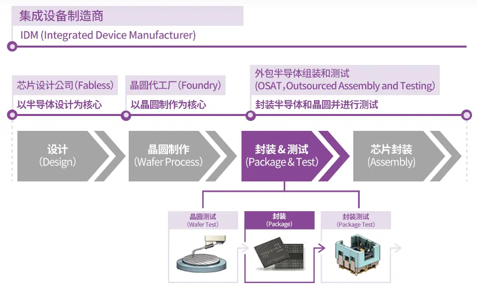
The above diagram illustrates the semiconductor manufacturing process and its industry segmentation. The operational model that focuses solely on semiconductor design is referred to as a fabless chip design company, with typical representatives including Qualcomm and Apple. Manufacturers responsible for wafer fabrication are known as foundries, which produce wafers based on designs from fabless companies. A prominent example of this is TSMC (Taiwan Semiconductor Manufacturing Company), while other Korean companies like DB HiTek and Magnachip also adopt this model. Wafers designed by fabless companies and manufactured by foundries must undergo packaging and testing, which are handled by companies specializing in outsourced semiconductor assembly and testing (OSAT), with typical representatives including ASE, JCET, Stats Chippac, and Amkor. Additionally, there are integrated device manufacturers (IDMs) like SK Hynix that encompass multiple segments of the semiconductor supply chain, including design, wafer fabrication, packaging, and testing.
As shown in the diagram, the first step in the packaging and testing process is wafer testing, followed by testing after packaging.
One of the main purposes of semiconductor testing is to prevent defective products from being shipped. If defective products are provided to customers, it significantly undermines their trust in us, which can lead to a decline in sales performance and potential financial losses due to compensation claims. Therefore, we must conduct thorough and detailed inspections of products before they leave the factory. Semiconductor testing must evaluate various parameters based on the product's characteristics to ensure quality and reliability. Of course, this requires investment in time, equipment, and labor, which in turn increases manufacturing costs. Consequently, many testing engineers are dedicated to reducing testing time and the number of testing parameters.
#2 Types of testing
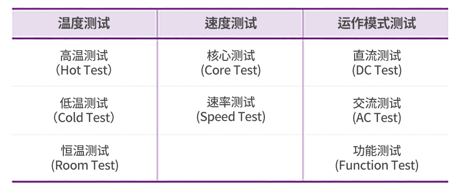
The testing process can be categorized based on different testing subjects into wafer testing and package testing; it can also be divided into three types based on different testing parameters: temperature testing, speed testing, and operational mode testing.
Temperature testing is based on the temperature applied to the test samples: in high-temperature testing, the temperature applied to the product exceeds the upper limit of the temperature range specified in the product specifications by 10%; in low-temperature testing, the applied temperature is 10% lower than the lower limit of the specifications; and the temperature applied in constant temperature testing is generally set at 25°C. In practical use, semiconductor products must operate in various environments, so it is essential to test the product's performance at different temperatures and its temperature margin. For example, in semiconductor memory, the high-temperature testing range is typically 85-90°C, while the low-temperature testing range is -5 to -40°C.
Speed testing is further divided into core testing and rate testing. Core testing primarily assesses the core operation of the test sample, specifically whether it can successfully achieve the intended functional goals. For semiconductor memory, since its main function is information storage, the focus of testing is on the parameters related to the information storage units. Rate testing measures the operational speed of the sample to verify whether the product can operate at the target speed. With the increasing demand for high-speed semiconductor products, rate testing is becoming increasingly important.
Operational mode testing is subdivided into DC testing, AC testing, and functional testing: DC testing verifies the parameters of direct current and voltage; AC testing verifies the specifications of alternating current, including the input and output transition times and other operational characteristics; functional testing verifies whether the logical functions operate correctly. For semiconductor memory, functional testing refers to testing whether the memory cells and the surrounding circuit logic function properly.
#3 Wafer Testing
Wafer testing targets the wafer, which consists of many chips, and the purpose of testing is to examine the characteristics and quality of these chips. To achieve this, wafer testing requires connecting the testing machine to the chips and applying current and signals to them.
Once the product is packaged, it forms pins similar to solder balls, which allow for easy electrical connection with the testing machine. However, in the wafer state, connecting the two requires special methods, such as using a probe card.
As shown in Figure 2, the probe card serves as the interface between the wafer being tested and the testing machine. The card is equipped with many probes that can directly connect the testing machine's communication interface to the wafer's pads. Additionally, the card contains numerous connecting wires that link the probes to the testing machine. The probe card is fixed to the test head, and the wafer probe station completes the testing by ensuring precise contact between the probe card and the wafer pads.
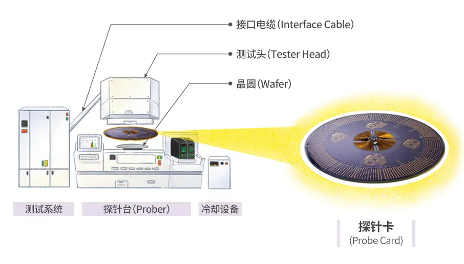
After loading the wafer with the front side facing up, the probe card on the right side of Figure 2 is flipped over so that the probe tips face down, achieving precise alignment with the wafer pads. At this point, the temperature control equipment applies the corresponding temperature based on the required testing conditions. The testing system transmits current and signals through the probe card and extracts chip signals to read the test results.
The probe card must be designed according to the pad layout of the chip being tested and the arrangement of the wafer chips, meaning that the probes must align with the pads on the wafer. Additionally, the probes need to be arranged repeatedly according to the chip layout. In practice, it is not possible to test all the chips on the wafer with just one contact. Therefore, in actual mass production, multiple contacts (typically 2 to 3 times) are necessary.
Generally speaking, wafer testing is conducted in the following sequence: Electrical Parameter Monitoring (EPM) → Wafer Burn-in → Testing → Repair → Testing.
#4 Package Testing
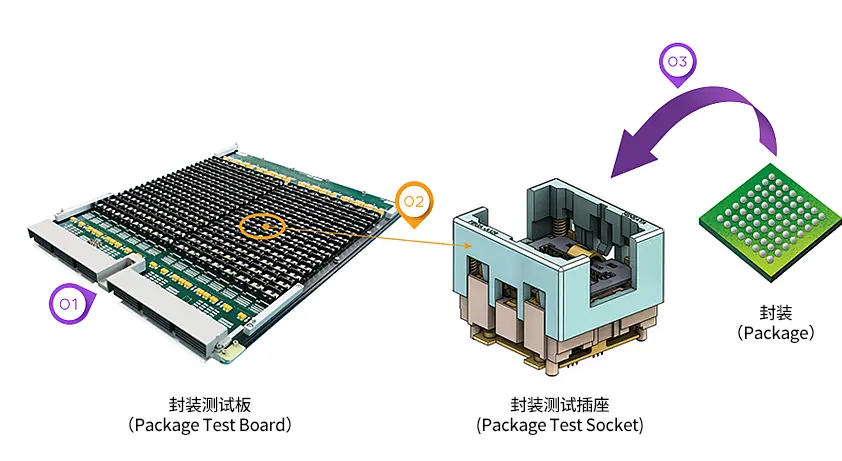
Chips that are deemed good during wafer testing need to undergo package testing after the packaging process, as issues may arise during packaging. Additionally, since wafer testing evaluates multiple chips simultaneously, limitations in the testing equipment’s performance may prevent it from fully testing the target parameters. In contrast, package testing is conducted on a per-package basis, which places a relatively lower load on the testing equipment and allows for comprehensive testing of the target parameters, thereby identifying good products that meet specifications.
The package testing method is illustrated in Figure 4: First, the package pins (Pins, shown as solder balls in the figure) are inserted into the package testing socket with the pins facing down, aligning them with the pins inside the socket. The package testing socket is then secured to the package test board for testing.
Contact Us
For any questions regarding our products or solutions, kindly entrust them to us and we will respond within 24 hours.
KeyWords
Wedge Bonding ToolWedge Tool
Bonding Wedge
Au Wire Bonding
Concave wedge Tool
Wedge Bonding Machines
Wire Bonding ToolsBonding Equipment SuppliersFine Pitch Bonding ToolsWedge BonderWire bonding equipmentSemiconductor bonding toolsPrecision bonding toolsHigh-performance wire bonding toolsSemiconductor industry toolsBonding tool manufacturerCustomizable wire bonding solutionsQuality wedge bonding equipment