

Hybrid Bonding: A Key Technology Leading the Future Development of the Semiconductor Industry
AI Systems and the Demands of the Post-Moore Era: Computing Power Stacking and Inter-Chip Data Transmission
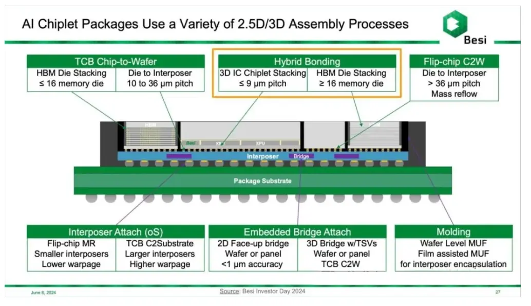
In recent years, the demand for AI chips has surged. Due to the complexity of large language models, a single chip cannot accommodate the entire model, leading AI chips to gradually evolve into systematic designs. AI systems typically consist of multiple computing chips (such as CPUs, GPUs, and ASICs) and memory chips (such as HBM). To enhance the performance of AI systems and reduce energy consumption, system designers need to place chips that require extensive data communication closer together, even adopting 2.5D or 3D packaging for interconnection. This interconnection not only accelerates transmission speeds but also reduces energy consumption, making advanced packaging play a vital role in an era where system energy consumption is increasingly important.
The Evolution of Packaging Technology: From Wire Bonding to Hybrid Bonding
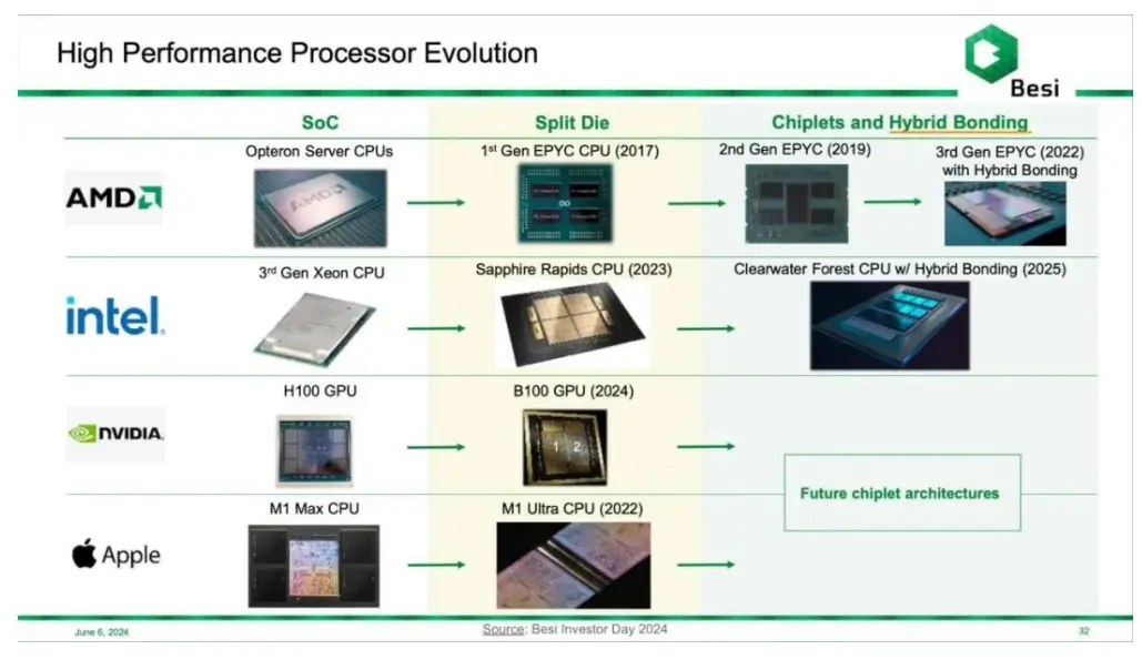
Packaging technology is continuously advancing towards advanced packaging, evolving from Wire Bonding to Die Bonding, and now to Hybrid Bonding. With the explosive demand for computing power in AI systems, major manufacturers have begun to stack chips aggressively, introducing advanced packaging technologies into AI chip systems. 2.5D packaging utilizes Micro bump technology, while systems requiring higher memory and CPU/GPU data transmission speeds adopt 3D Hybrid Bonding technology.
Hybrid Bonding Technology is Widely Applied, Not Limited to Logic Chip Stacking
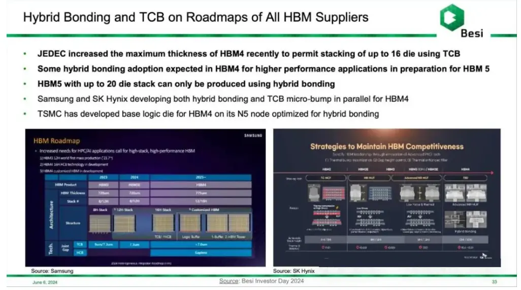
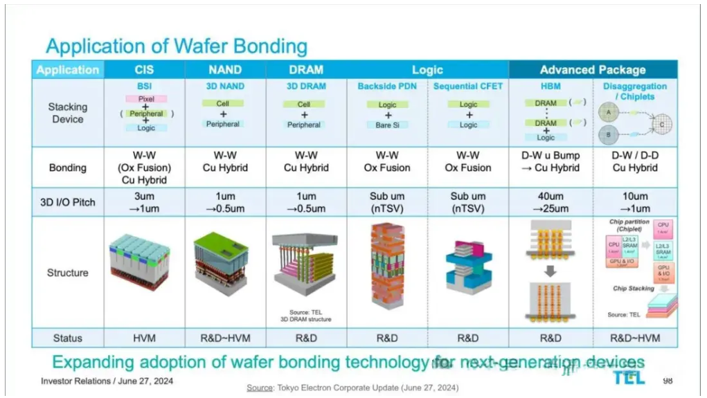
Hybrid Bonding technology is not only used in 3D packaging but is also widely applied in fields such as CMOS image sensors (CIS), 3D NAND, and HBM. HBM4 (the fourth generation of high bandwidth memory) may partially utilize Hybrid Bonding, while HBM5 will require Hybrid Bonding to meet performance demands. As a technology for connecting different chips or modules, Hybrid Bonding can significantly enhance data transmission speeds, and its importance will increasingly become prominent.
Principles and Advantages of Hybrid Bonding Technology
Hybrid Bonding is a wafer bonding technology that achieves interconnection between chips by forming direct copper-to-copper (Cu-Cu) bonds between wafers. Compared to traditional bonding technologies, Hybrid Bonding offers the following advantages:
-
Smaller Bonding Pitch: Hybrid Bonding can achieve a smaller bonding pitch, thereby increasing the interconnection density between chips and enhancing chip performance.
-
Lower Resistance: Due to the low resistance of copper-to-copper bonding, Hybrid Bonding can reduce signal transmission delays between chips, improving chip speed.
-
Higher Reliability: The bonding strength of Hybrid Bonding is high, which can enhance the reliability of the chips.
-
Lower Power Consumption: With lower resistance, Hybrid Bonding can reduce power consumption between chips.
-
The Importance of Hybrid Bonding Technology for Future AI Systems
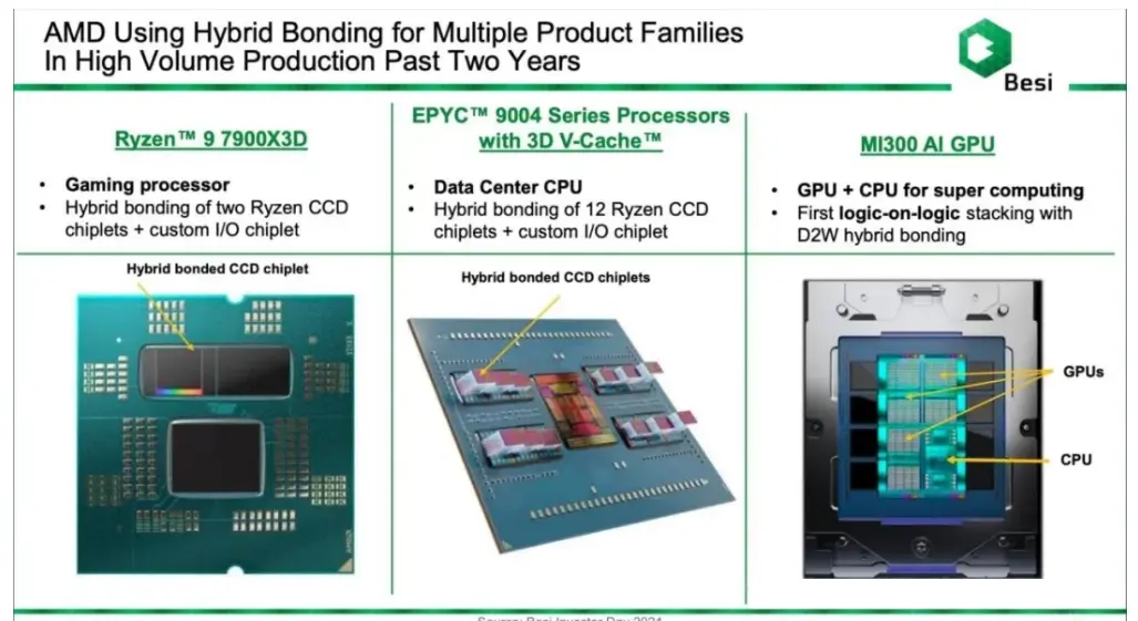
Although the application of Hybrid Bonding technology in current AI chips is still limited, the future demand for computing power will drive more chip stacking, significantly increasing the data transmission requirements between chips. Additionally, the energy consumption of multi-chip systems will need to be more efficient. Therefore, Hybrid Bonding technology will play an important role in AI chip systems, whether in 3D packaging or in the manufacturing of the next generation of HBM. The development of AMD’s AI GPU (MI300 and next-generation chips) also confirms this trend.
-
Conclusion
As an advanced chip bonding technology, Hybrid Bonding will play a key role in the future development of the semiconductor industry. With the rapid advancement of fields such as AI and high-performance computing, the demands for chip performance and power consumption are continuously increasing. Hybrid Bonding technology will provide strong support to meet these needs. We look forward to seeing the application of Hybrid Bonding technology in more areas, bringing further innovation and breakthroughs to the semiconductor industry.
Contact Us
For any questions regarding our products or solutions, kindly entrust them to us and we will respond within 24 hours.
KeyWords
Wedge Bonding ToolWedge Tool
Bonding Wedge
Au Wire Bonding
Concave wedge Tool
Wedge Bonding Machines
Wire Bonding ToolsBonding Equipment SuppliersFine Pitch Bonding ToolsWedge BonderWire bonding equipmentSemiconductor bonding toolsPrecision bonding toolsHigh-performance wire bonding toolsSemiconductor industry toolsBonding tool manufacturerCustomizable wire bonding solutionsQuality wedge bonding equipment