Leave Your Message

2026 Top Die Pick and Place Machine Types

In 2026, the top Die Pick and Place Machine Types reflect faster packaging, tighter tolerances, and more demanding semiconductor designs. Manufacturers now compare throughput, placement accuracy, die size, and process flexibility before choosing equipment. The right machine should match the package, wafer format, adhesive method, and production volume. Small differences matter. A few microns can affect alignment, bonding strength, and final yield.

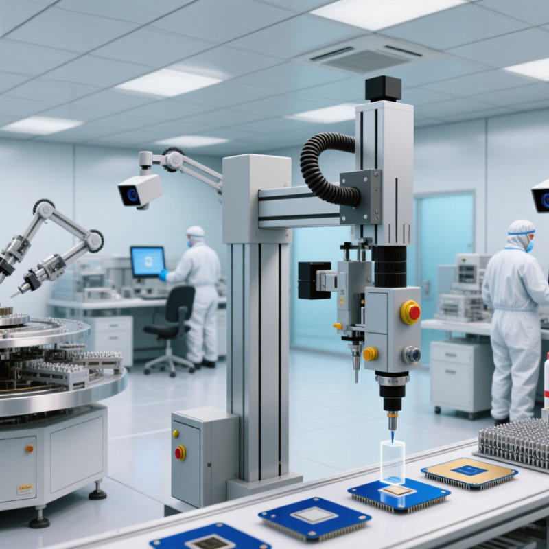
This guide examines how Die Pick Up And Place systems work across common assembly environments. It considers high-speed rotary platforms, precision gantry machines, flip-chip handlers, and flexible systems for advanced packaging. Each type has practical strengths. Rotary equipment may support continuous output, while gantry systems often provide controlled movement and easier recipe changes. Vision cameras inspect die edges, surface marks, and placement coordinates. Operators also need clear access to feeders, ejector needles, and maintenance areas.

Real production results depend on more than advertised speed. Cleanroom conditions, operator training, software stability, and material handling can change performance. No ranking is perfect. A machine that excels in a laboratory may struggle beside a busy bonding line. That point deserves attention. Buyers should validate sample wafers, test actual die geometries, and review service response before making a decision. Reliable evaluation combines supplier documentation, factory trials, maintenance records, and measured yield data. This balanced approach can reduce risk and support a practical investment for 2026.

2026 Top Die Pick and Place Machine Types

Die Pick and Place Machines: Definition and Core Functions

A die pick and place machine transfers individual semiconductor dies from a wafer, film frame, or tray onto a substrate. It combines wafer mapping, die ejection, optical inspection, gripping, alignment, and controlled placement. The machine must protect fragile surfaces while maintaining micron-level accuracy. Small errors can later become electrical failures.

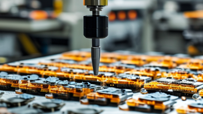
Core operation follows a measured sequence. A vision system identifies the die position and checks orientation. An ejector needle lifts the die, while a collet or bonding head picks it up. The placement head then aligns the die with substrate marks. Adhesive dispensing, pressure control, and heating may follow. Some systems handle flip-chip placement, while others support conventional die attach, stacked dies, or high-throughput rotary transfer. The distinction matters. Speed alone does not define productivity.

SEMI reported global semiconductor manufacturing equipment billings of 117.7 billion dollars in 2024, showing the scale of continuing factory investment. Grand View Research estimates that semiconductor assembly and packaging equipment will expand at about 8.6% annually through 2030. These figures support demand for more capable placement platforms, but they do not guarantee better production. Real performance depends on yield, changeover time, vacuum stability, and operator experience. A machine can place thousands of dies per hour and still waste material through poor calibration. That lesson is often underestimated.

Key Machine Types Used in Die Handling and Placement

2026 Top Die Pick and Place Machine Types

Key Machine Types Used in Die Handling and Placement

Die handling depends on accuracy, speed, and surface protection. The main machine types include vacuum pick-and-place systems, collet-based handlers, flip-chip placement machines, and robotic transfer units. Vacuum tools suit flat dies with clean, stable surfaces. Collets offer firmer control when dies are small, thin, or slightly uneven. Flip-chip systems add controlled rotation and alignment for bump-based placement. Robotic transfer units work well when dies move between trays, inspection stations, and placement platforms.

Each machine has a practical role. High-speed pick-and-place equipment supports large production volumes, while precision bonders focus on micron-level alignment. Vision systems inspect die edges, orientation, and placement coordinates before bonding. Experienced technicians also check tool wear, vacuum pressure, and tray flatness during routine operation. Small errors become expensive quickly.

Tips: Match the tool to the die material and geometry. Test pickup force on sample dies before full production. Keep the work surface clean. A few particles can change placement height. Record rejected dies and review the pattern daily. This simple habit often reveals unstable vacuum, poor alignment, or handling damage. No machine is perfect. Even a well-calibrated system may need slower motion for fragile dies, and that trade-off can be easy to overlook.

How Each Die Pick and Place Machine Operates

Die Pick and Place Machine Types: How Each Machine Operates

Die pick and place machines transfer individual semiconductor dies from wafer tape to a substrate, leadframe, or carrier. Their operation combines vision, vacuum handling, motion control, and placement force. A camera locates each die and checks its orientation. A collet then lifts the die from the tape. The motion stage follows a programmed path. Placement pressure must remain gentle. Excessive force can damage fragile edges or disturb the adhesive layer.

Standard adhesive die attach systems dispense epoxy or use adhesive film before placement. The collet lowers the die onto the bonding material, while sensors verify height and contact. Eutectic systems add controlled heating, often inside an inert environment, to form a metallic bond. They require stable temperature and clean surfaces. Flip-chip machines handle dies with bumps facing downward. Vision alignment matches the bumps with substrate pads, then controlled force completes contact. Thermal compression may follow.

Wafer-level and multi-die platforms modify the sequence for higher output. A wafer table maps approved dies, while software skips marked defects. Multi-head designs place several dies in one cycle, but synchronization becomes harder. Operators inspect pickup success, placement offset, tilt, and bond-line thickness. A fast cycle is not always reliable. Dust, tape variation, and imperfect calibration still create rejects. Regular nozzle cleaning, reference-die checks, and trend reviews help detect drift early. Machine manuals matter, but production evidence should challenge assumptions.

2026 Top Die Pick and Place Machine Types - How Each Die Pick and Place Machine Operates
Machine Type How It Operates Typical Die Handling Alignment Method Typical Placement Capability Best-Fit Applications Main Advantages Common Limitations
Standard Die Pick-and-Place Bonder A needle or ejector lifts the die from the wafer tape while a vacuum collet picks it up, moves it through a programmed path, and places it onto a lead frame, substrate, or adhesive layer. Small to medium silicon, compound-semiconductor, sensor, and power device dies; commonly used with diced wafers mounted on adhesive tape. Wafer-map recognition, substrate fiducials, pattern-recognition cameras, and calibrated X-Y-theta motion stages. Approximately 10–50 µm placement accuracy; up to several thousand placements per hour, depending on die size and process steps. Conventional die attach, discrete semiconductors, LED packages, sensors, and general semiconductor assembly. Flexible tooling, broad material compatibility, relatively simple process setup, and good suitability for high-volume production. Less suitable for extremely thin, fragile, warped, or very large dies without specialized ejector and handling systems.
High-Speed Turret or Rotary Die Bonder Multiple pick-and-place heads are arranged on a rotating turret. While one head picks a die, other heads can inspect, transfer, or place dies, allowing several operations to occur in parallel. Small, robust dies with consistent dimensions and repeatable pickup characteristics. Vision alignment combined with mechanically synchronized rotary stations and fixed transfer positions. Often above 5,000 placements per hour in optimized production; practical accuracy is commonly about 15–40 µm. High-volume discrete packages, LED products, small power devices, and applications with stable product designs. High throughput, short transfer distances, and efficient parallel operation. Reduced flexibility for frequent product changeovers, complex orientations, or wide die-size variation.
Flip-Chip Bonder The die is picked, rotated face-down, aligned to substrate bumps or pads through optical recognition, and placed with controlled force. Interconnection is then completed by reflow, thermocompression, or another bonding process. Bumped dies, micro-bumped dies, copper-pillar devices, and fine-pitch semiconductor components. Separate or through-the-tool optical systems observe die and substrate marks; some systems align both surfaces before placement. Approximately 1–10 µm alignment capability for advanced processes, depending on pitch, optics, motion stage, and bonding method. Advanced processors, memory, image sensors, radio-frequency devices, chip-scale packages, and heterogeneous integration. Supports fine-pitch interconnection, short electrical paths, and compact package designs. Higher equipment cost, demanding surface cleanliness, precise thermal control, and more complex process qualification.
Thermocompression Die Bonder A heated tool picks and places the die, then applies controlled heat, force, and dwell time to form direct metallic or bump-based interconnections. Thin dies, stacked memory components, copper-pillar assemblies, and fine-pitch devices requiring controlled compression. High-resolution vision alignment with force, temperature, and position feedback during bonding. Commonly about 1–5 µm alignment capability in advanced configurations; cycle time is affected by heating and compression dwell. 2.5D and 3D packaging, die stacking, fine-pitch chip assemblies, and advanced memory integration. Low solder volume, fine-pitch capability, and strong control of bond pressure and thermal profiles. Relatively long cycle times, thermal stress concerns, and demanding control of warpage and bonding surfaces.
Eutectic Die Attach Bonder The die is picked and aligned over a metalized bonding surface. Localized heating melts a eutectic alloy, such as a gold-tin or similar system, and the die is placed under controlled force before the joint solidifies. Power dies, laser or photonic dies, high-reliability devices, and components requiring efficient thermal transfer. Vision alignment using substrate fiducials, die edges, or optical reference marks. Typically about 5–20 µm placement accuracy, with process capability strongly influenced by die flatness and metallization quality. High-power electronics, optoelectronics, laser modules, and hermetic or high-temperature packages. Excellent thermal and mechanical performance with low bond-line thickness and high long-term reliability. Requires compatible metallization, controlled atmosphere or flux management, and precise temperature control.
Adhesive Die Attach Machine A dispensing or pre-applied adhesive layer is prepared on the substrate. The pick head places the die onto the adhesive, and the assembly is cured by heat, ultraviolet light, or a combination of curing methods. Silicon, ceramic, compound-semiconductor, and optoelectronic dies; suitable for many die sizes and substrate materials. Camera-based recognition of die edges and substrate fiducials, usually combined with controlled placement force. Approximately 10–50 µm placement accuracy; throughput varies widely with adhesive dispensing and curing requirements. General semiconductor packaging, sensors, LEDs, modules, and applications requiring electrical isolation. Broad adhesive choice, relatively low process temperature, and good compatibility with dissimilar materials. Cure shrinkage, adhesive voids, outgassing, bond-line variation, and longer total process time may affect yield.
Soft-Handling Thin-Die Bonder A low-stress ejector, compliant vacuum collet, or specialized membrane-assisted tool separates and transfers thin dies while minimizing bending, edge chipping, and surface damage. Thin, flexible, large-area, fragile, or low-k semiconductor dies, including dies with delicate surface structures. Vision alignment with controlled Z motion, low pickup force, and force or vacuum monitoring. Commonly about 10–30 µm placement accuracy; handling performance is often more critical than maximum placement speed. Thin wafers, stacked-die packages, flexible devices, sensors, and advanced mobile or wearable components. Reduces die cracking, backside damage, edge chipping, and handling loss during transfer. Lower throughput, specialized tooling requirements, and greater sensitivity to wafer tape, die flatness, and contamination.
Multi-Die or Die-Stacking Bonder The machine repeatedly picks and places several dies on the same package or directly stacks them. Vision systems verify each layer, while height, tilt, force, and adhesive or interconnect conditions are monitored. Memory dies, logic-and-memory combinations, sensor stacks, and vertically integrated multi-chip assemblies. Fiducial recognition, die-edge inspection, 3D height measurement, and interlayer alignment verification. Approximately 2–15 µm layer-to-layer alignment, depending on package architecture and interconnect pitch. 3D integrated packages, high-bandwidth memory assemblies, stacked sensors, and compact multi-chip modules. Enables high functional density, reduced package footprint, and integration of different semiconductor technologies. Cumulative alignment error, die warpage, thermal management, and process control become increasingly challenging as stack height grows.
Wafer-Level Die Transfer System Dies are transferred from one wafer, carrier, or temporary tape surface to another substrate or panel using coordinated wafer mapping, mass-transfer, or sequential pick-and-place operations. Very small dies, micro-LED elements, sensor arrays, and devices requiring organized transfer across large areas. Wafer mapping, global and local fiducials, high-magnification vision, and synchronized wafer-to-substrate coordinate transformation. Approximately 2–20 µm placement accuracy; throughput depends heavily on die size, transfer architecture, and inspection requirements. Wafer-level packaging, micro-display production, sensor arrays, and large-area electronic assemblies. Efficient use of wafer maps, scalable substrate transfer, and strong compatibility with automated inspection and traceability. Complex calibration, substrate distortion, carrier management, and demanding uniformity requirements across large working areas.
Note: Accuracy and throughput figures are typical industry ranges rather than guaranteed specifications. Actual performance depends on die size, wafer thickness, bonding material, package geometry, vision configuration, process tolerances, and inspection requirements.

Performance Factors for Comparing Machine Types in 2026

2026 Top Die Pick and Place Machine Types

Performance Factors for Comparing Machine Types in 2026

Demand is rising, but speed alone should not decide a die pick and place machine. The WSTS Spring 2025 forecast projects the semiconductor market will reach about 746 billion dollars in 2026. That growth increases pressure on yield, uptime, and flexible production.

Compare machines by verified throughput, placement accuracy, and usable uptime. A high-speed rotary system may suit stable, high-volume die packages. A flexible linear platform can perform better with frequent product changes. Check accuracy at production temperature, not only in laboratory conditions. Vision resolution, ejector control, bonding-force stability, and wafer-map handling also matter. SEMI’s 2024 World Fab Forecast projected global fab capacity growth of approximately 7% in 2025. More capacity will not help if changeover takes hours or operators frequently correct alignment errors. That point is easy to overlook.

Tips: Request a three-shift acceptance test. Measure good units per hour, not advertised cycles per hour. Record stoppage reasons, setup time, scrap, and recovery time. Ask for data from similar die sizes and substrate materials. Energy use and maintenance access deserve attention too. Small maintenance delays become expensive at scale. My practical concern is this: comparison tables often hide process variation. A machine may look weaker on peak speed, yet deliver more saleable units each day. Validate the result with your own die, adhesive, substrate, and operators.

Selecting the Right Die Pick and Place Machine for Production Needs

2026 Top Die Pick and Place Machine Types

Selecting the right die pick and place machine starts with the production task, not catalog speed. Manual systems suit prototypes, engineering samples, and low-volume work. Semi-automatic machines improve repeatability while keeping changeovers relatively simple. Fully automatic systems support high-volume lines with integrated vision, wafer handling, and closed-loop placement control.

Match the machine to die size, thickness, weight, and surface sensitivity. A fragile die may need soft vacuum tooling, controlled acceleration, and precise release timing. Check placement accuracy under real operating conditions, not only laboratory specifications. Cycle time also depends on feeder loading, inspection, operator movement, and product changeovers. Small details matter.

Think beyond today’s order forecast. A modular platform can accommodate new packages, but unused capacity increases purchase and maintenance costs. In line assessments, engineers should measure actual reject causes, alignment drift, and tool replacement time. A higher-rated speed is not always better. It may create more vibration or reduce handling stability. No selection is perfect. Our first estimate can be wrong, especially when sample data is limited. Run representative trials with production materials, record the results, and let operators challenge the assumptions before final approval.