Why is Automatic Wire Bonder Essential for Advanced Semiconductor Packaging
As the landscape of semiconductor packaging continues to evolve, the role of technologies such as the Automatic Wire Bonder has become increasingly crucial. This advanced machinery is at the forefront of enabling higher precision and efficiency in the interconnection of semiconductor devices. According to Dr. Emily Wu, a leading expert in semiconductor manufacturing, "The Automatic Wire Bonder is not just a tool; it's an essential instrument that drives innovation in semiconductor packaging by ensuring robust connections at micro-level."
In today’s market, where performance and miniaturization are paramount, the Automatic Wire Bonder offers solutions that meet the rising demands for compact and reliable electronic components. Its ability to handle various wire types and configurations allows engineers to design more intricate packages, ultimately enhancing the functionality of devices that power our modern world. As industries from consumer electronics to automotive sectors push for more integrated solutions, the significance of the Automatic Wire Bonder becomes even more pronounced.
Moreover, the evolution of packaging technologies necessitates a shift towards automation and precision. Automatic Wire Bonders not only streamline the manufacturing process but also reduce the margin of error associated with manual bonding techniques. This transition is vital for maintaining the competitiveness and reliability of semiconductor components in a fast-paced technological environment. As we delve deeper into the role of Automatic Wire Bonders in advanced semiconductor packaging, it becomes evident that these machines represent the backbone of future innovations in the electrical engineering landscape.
The Role of Automatic Wire Bonders in Semiconductor Packaging
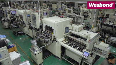
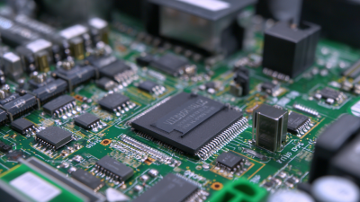
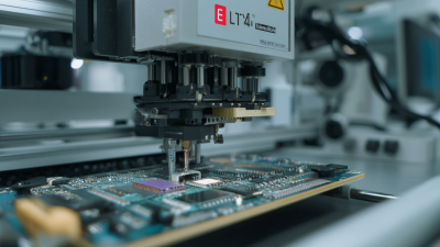
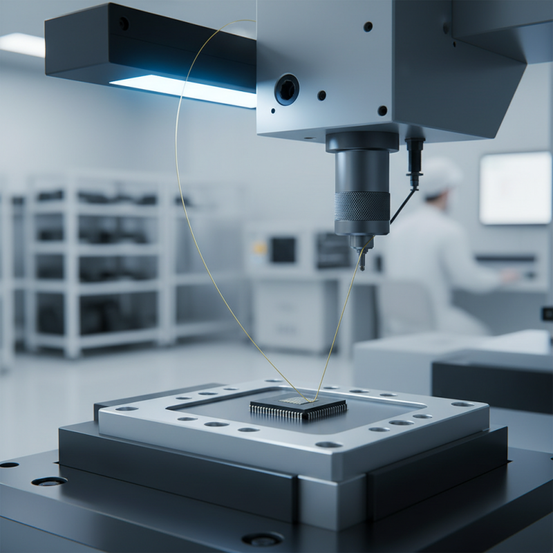
Automatic wire bonders play a critical role in the semiconductor packaging process, serving as a vital link between the chip and the external circuitry. By facilitating the precise attachment of fine wires from the semiconductor die to the lead frame, these machines ensure robust electrical connections essential for the functionality of modern electronic devices. As technology progresses, the demand for more compact designs and increased performance levels has propelled the evolution of wire bonding techniques, making automatic wire bonders indispensable in advanced packaging methodologies.
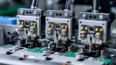
Moreover, the flexibility and efficiency offered by automatic wire bonders significantly enhance production capabilities. These machines are equipped with advanced algorithms and controls that allow for high-speed operations, reducing cycle times and improving output quality. The integration of automation also minimizes human error and enhances repeatability, which are crucial in maintaining production standards in semiconductor manufacturing. As semiconductor manufacturers face the challenges of miniaturization and higher performance requirements, the indispensable role of automatic wire bonders becomes increasingly evident in ensuring the reliability and efficiency of semiconductor packages.
Key Advantages of Using Automatic Wire Bonders
The advancement of semiconductor packaging technology has necessitated the adoption of automatic wire bonders. These machines play a crucial role in enhancing the efficiency and reliability of the packaging process. According to a recent industry report, the global market for wire bonding equipment is projected to reach $4.5 billion by 2025, driven by the growing demand for high-performance semiconductors in applications such as 5G technology and artificial intelligence. Automatic wire bonders provide unparalleled precision, allowing manufacturers to achieve tighter bonding pitches and consistent quality, which are essential for advanced packaging designs.
One of the key advantages of using automatic wire bonders is their ability to increase production throughput. With automation, the process can run continuously with minimal human intervention, significantly reducing cycle times. A study indicates that utilizing automatic wire bonding can improve production efficiency by up to 30%, which is critical in meeting the escalating demands of the semiconductor industry. Additionally, these machines are equipped with sophisticated monitoring and control systems that enhance yield rates by detecting and correcting potential issues in real-time, leading to fewer defects and reliable performance in the final product.
Furthermore, automatic wire bonders contribute to cost-effectiveness in semiconductor packaging. By minimizing material waste and labor costs, they help manufacturers maintain competitive pricing without sacrificing quality. The integration of advanced technologies such as machine learning and AI into these systems also allows for continuous optimization of the bonding process, ensuring that manufacturers remain at the forefront of innovation in an ever-evolving market.
Why is Automatic Wire Bonder Essential for Advanced Semiconductor Packaging - Key Advantages of Using Automatic Wire Bonders
| Feature |
Description |
Benefit |
| Precision |
High accuracy in wire placement |
Improves signal integrity and reliability |
| Speed |
Faster bonding process compared to manual methods |
Increases overall production throughput |
| Automation |
Fully automated operation reduces human error |
Enhances consistency in production quality |
| Versatility |
Ability to bond various wire types and sizes |
Accommodates a wide range of semiconductor packaging |
| Cost Efficiency |
Reduced labor costs and material waste |
Lowered production costs and improved profit margins |
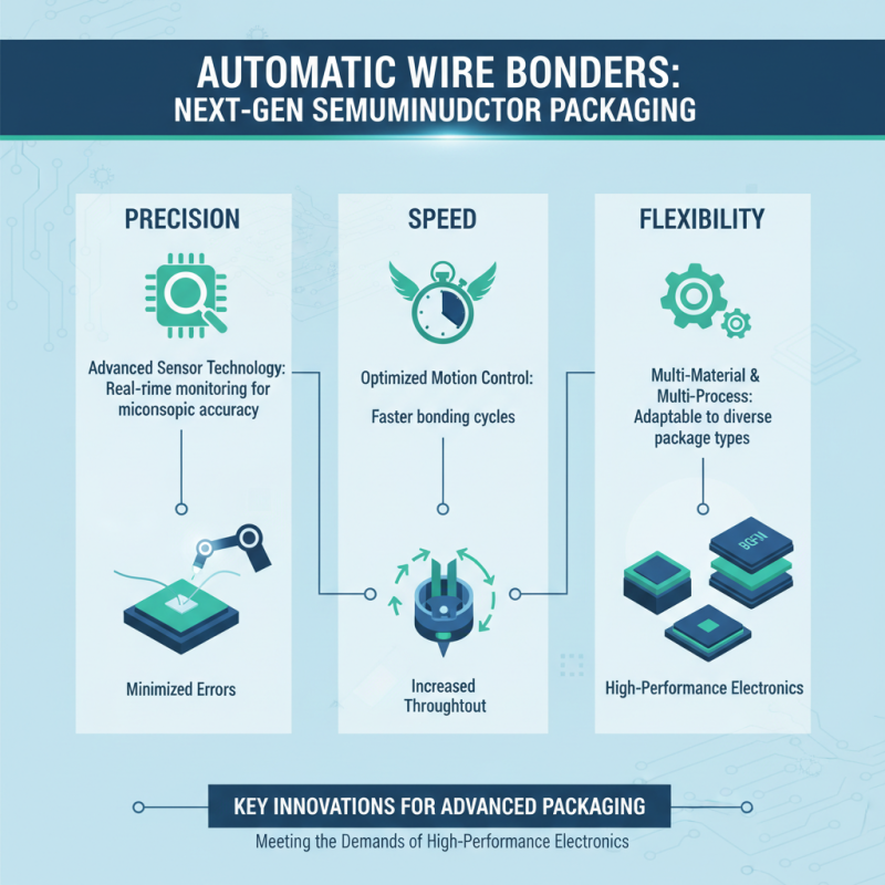
Technological Innovations in Automatic Wire Bonders
Automatic wire bonders have witnessed significant technological innovations that enhance their role in advanced semiconductor packaging. These innovations focus on improving precision, speed, and flexibility in the bonding process, essential for meeting the growing demands of high-performance electronics. Advanced sensor technology, for instance, allows for real-time monitoring of the bonding process, ensuring optimal performance and minimizing errors. This capability is crucial in the fabrication of smaller and more complex semiconductor packages that require meticulous attention to detail.
Moreover, the integration of artificial intelligence and machine learning into automatic wire bonders has revolutionized their operational efficiency. By analyzing data from previous bonding processes, these systems can adapt to various materials and designs, optimizing parameters for each unique application. This adaptability not only enhances productivity but also allows manufacturers to implement novel packaging techniques that were previously difficult to achieve. As semiconductor technology continues to evolve, the advancements in automatic wire bonders play a pivotal role in pushing the boundaries of what is possible in semiconductor packaging, enabling the development of smaller, faster, and more efficient electronic devices.
Challenges Addressed by Automatic Wire Bonders in Packaging
Automatic wire bonders play a crucial role in addressing the challenges faced in advanced semiconductor packaging. As semiconductor devices become increasingly complex, the demand for higher interconnect density and improved performance is paramount. One significant challenge is the need for precise and reliable bonding of fine wires to both the chip and package substrate. Automatic wire bonders enhance precision and consistency, ensuring that the bonds can withstand the rigors of thermal and mechanical stresses experienced during operation.
Additionally, the shift towards smaller, more efficient forms of packaging has created obstacles in maintaining the delicate balance between size and performance. Automatic wire bonders are designed to adapt to these shrinking dimensions while providing accurate placement and minimal wire sweep. Their automated capabilities reduce human error and increase throughput, addressing the industry's continuous need for high-volume production without compromising quality. As the complexity of semiconductor applications escalates, these bonders offer innovative solutions that meet the advanced requirements of modern packaging technologies.
Challenges Addressed by Automatic Wire Bonders in Advanced Semiconductor Packaging
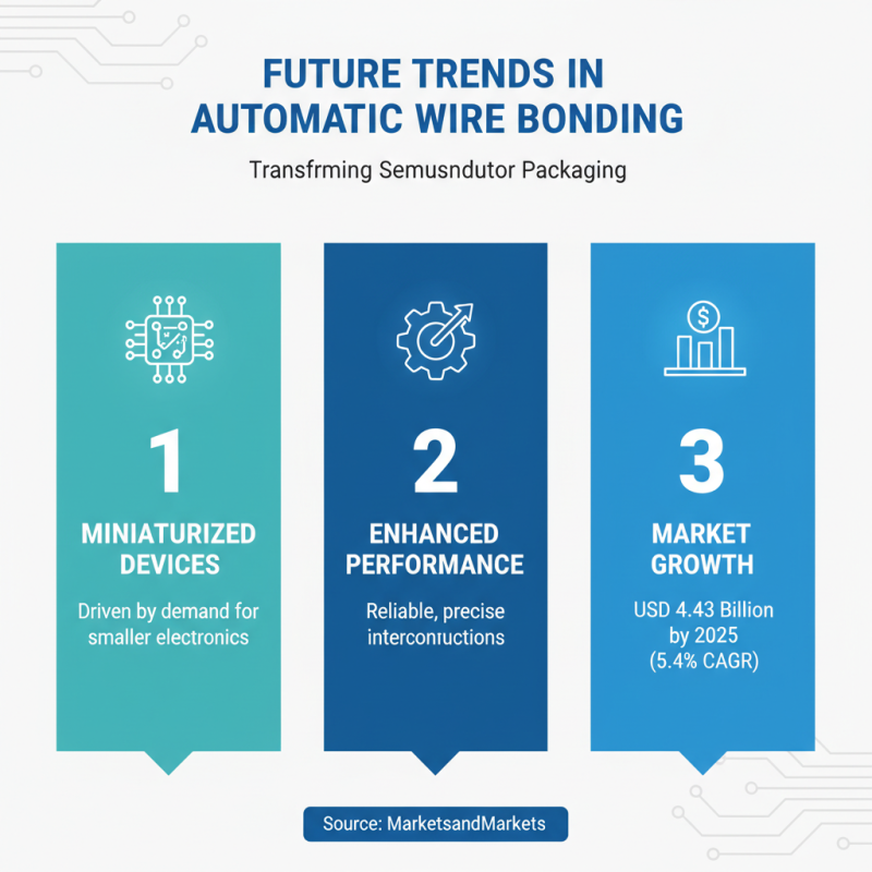
Future Trends in Automatic Wire Bonding Technology
The future trends in automatic wire bonding technology are poised to transform the landscape of semiconductor packaging, driven by the increasing demand for miniaturized electronic devices and enhanced performance capabilities. As reported by MarketsandMarkets, the wire bonding market is expected to reach USD 4.43 billion by 2025, growing at a CAGR of 5.4%. This growth is primarily fueled by advancements in automation, which allow for the precise and reliable interconnection of chips in complex packaging environments.
One of the most significant trends is the integration of artificial intelligence (AI) and machine learning in the wire bonding process. With the ability to analyze data in real time, these technologies can optimize bonding parameters, reduce defects, and minimize cycle times. Furthermore, the adoption of advanced materials, such as low-loop wire bonds and fine-pitch applications, is enhancing the performance of wire bonding, especially in high-frequency and high-temperature environments. According to a report by IDTechEx, the use of advanced materials in semiconductor packaging reduces assembly errors and improves overall device reliability.
Moreover, the rise of emerging applications like Internet of Things (IoT) devices and automotive electronics is driving innovation in bonding techniques. These applications require robust and scalable bonding solutions that can meet the rigorous demands of modern electronics. As highlighted by Yole Développement, the increasing complexity of semiconductor devices necessitates the development of more sophisticated wire bonding equipment capable of achieving greater accuracy and efficiency, ensuring that manufacturers can keep pace with the rapid evolution of technology in the coming years.